
In0.53Ga0.47As MOSFETs with high channel mobility and gate stack quality fabricated on 300 mm Si substrate
In 0.53 Ga 0.47 As channel MOSFETs were fabricated on 300 mm Si substrate. The epitaxial In 0.53 Ga 0.47 As channel layer exhibits high Hall electron mobility comparable to those grown on lattice matched InP substrates. Excellent device characteristics (SS~95 mV/dec., I on /I off ~10 5 , DIBL ~51 mV/V at V ds = 0.5V for L g =150 nm device) with good uniformity across the wafer were demonstrated. The extracted high field effect mobility (μ EF = 1837 cm 2 /V-s with EOT ~ 0.9 nm) is among the highest values reported for surface channel In 0.53 Ga 0.47 As MOSFETs.
Germanium-based Transistors for Future High Performance and Low Power Logic Applications
High mobility channel materials could replace strained Si to enhance speed performance and/or reduce power consumption in future transistors. Ge has the highest hole mobility among common elemental and compound semiconductors, and an electron mobility that is two times larger than that of Si. Ge is thus a promising channel material for future CMOS (Fig. 1). Key challenges include cost-effective integration of Ge on Si in a manufacturable process, formation of high-quality gate stack on Ge for n- and p-FETs at aggressively scaled EOTs that deliver high channel mobilities, and leakage issues related to its small bandgap. In this paper, we discuss recent research progress in advancing Ge-based transistor technologies. Integration of Ge on Si substrate to enable fabrication of high performance devices and formation of high-quality gate stack for Ge FETs (particularly for n-FETs) will be discussed. We also explore opportunities to boost the mobility of Ge, e.g. by incorporating Sn in Ge to form Ge 1-x Sn x . Furthermore, by raising the Sn composition, the band gap E G of Ge 1-x Sn x becomes smaller and transits from indirect to direct, making Ge 1-x Sn x a promising material for tunneling transistors.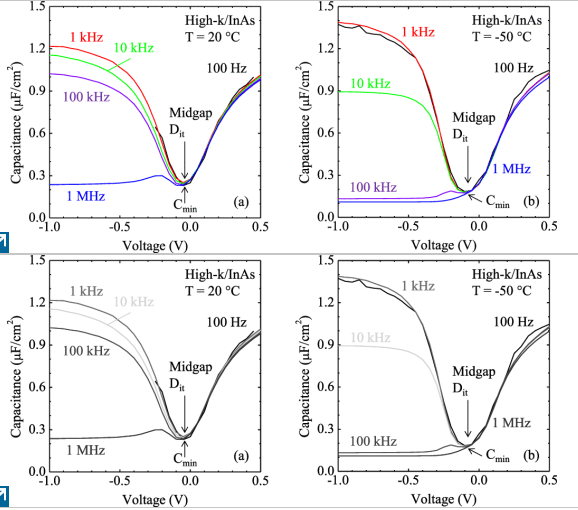
Field-Effect Mobility of InAs Surface Channel nMOSFET With Low Dit Scaled Gate-Stack
Frequency (100 Hz ≤ f ≤ 1 MHz) and temperature (-50 ≤ T 20 °C) characteristics of low interface state density D it high-κ gate-stacks on n-InAs have been investigated. Capacitance-voltage (C-V) curves exhibit typical accumulation/depletion/inversion behavior with midgap D it of 2 × 10 11 and 4 × 10 11 cm -2 eV -1 at -50 °C and 20 °C, respectively. Asymmetry of low-frequency C-V curves and C-T dependence for negative voltage showing a sharp transition of ≅-20 dB/decade between low- and high-frequency behavior indicate surface inversion. An inversion carrier activation energy and an InAs hole lifetime of 0.32 eV and 2 ns have been extracted, respectively. Surface channel nMOSFETs with gate length L g = 1 μm, channel thickness = 10 nm, and equivalent oxide thickness (EOT) 1 ≤ EOT ≤ 1.6 nm have been fabricated. For EOT = 1 nm, a subthreshold swing S = 65 mV/decade, transconductance g m = 1.6 mS/μm, and ON-current I ON = 426 μA/μm at an OFF-current I OFF = 100 nA/μm (supply voltage V dd = 0.5 V) have been measured. Peak electron field-effect mobilities of 6000-7000 cm 2 /Vs at sheet electron densities of 2-3 × 10 12 cm -2 were obtained for EOT as small as 1 nm.
Germanium n-Channel Planar FET and FinFET: Gate-Stack and Contact Optimization
We demonstrate Ge enhancement-mode nMOS FinFETs fabricated on 300-mm Si wafers, incorporating an optimized gate-stack (interface trap density D it below 2 × 10 11 eV -1 · cm -2 ), n + -doping (active doping concentration Nact exceeding 1 × 10 20 cm -3 ), and metallization (contact resistivity Pc below 2 × 10 -7 Ω · cm 2 ) modules. A new circular transmission line Pc extraction model that captures the parasitic metal resistance is proposed. At a supply voltage VDD of 0.5 V, 40-nm-gate-length FinFET devices achieved an ON-performance ION of 50 μA/μm at an OFF-state current IOFF of 100 nA/μm, a subthreshold swing S sat of 124 mV/decade, and a peak transconductance g m of 310 μS/μm. The same gate-stack and contacts were deployed on planar devices for comparison. Both FinFET and planar devices in this paper achieved the highest reported g m /S sat at VDD = 0.5 V to date and the shortest gate lengths for Ge nMOS enhancement-mode transistors.
AlxIn1−xAsySb1−y alloys lattice matched to InAs(1 0 0) grown by molecular beam epitaxy
AlxIn1−xAsySb1−y quaternary alloys lattice-matched to InAs were successfully grown by molecular beam epitaxy (MBE) for use as buffer layers for substrate isolation in InAs channel devices. The use of In-containing quaternary buffer layers with 5% In was found to dramatically improve the heterointerface between the buffer and a surface InAs channel layer. The composition of these alloys and the extent of lattice matching were accurately determined by double crystal X-ray measurements. A simple model was used to estimate the variation of critical thickness with lattice mismatch for AlInAsSb epitaxially grown on an InAs substrate. Layers with high Al content and low As mole fraction were grown by modulated MBE technique which was found to significantly improve the surface morphology and the composition control of the alloys. In contrast, quaternary alloys with low Al content were grown by conventional MBE and had an rms roughness of less than 0.2 nm.
Ab initio study of dipole-induced threshold voltage shift in HfO2/Al2O3/(100)Si
The ab initio work quantitatively explains the physical mechanism of threshold voltage shifts in n-type and p-type metal-oxide-semiconductor field-effect transistors with HfO 2 /Al 2 O 3 gate stack. In the study, the θ phase alumina has been chosen for better lattice matching of the (100) HfO 2 and (100) Si substrate. Using dipole correction method, the dominant dipole moment responsible for the threshold voltage shift has been identified at the interface of HfO 2 /Al 2 O 3 . Our HfO 2 /Al 2 O 3 atomic model shows the dipole moment decreases almost linearly as the alumina thickness decreases from four monolayers (13 Å) to one monolayer (3 Å). On account of the effects of capacitance and the dipole moment, our ab initio calculation quantitatively explains the trend and sensitivity of experimental threshold voltage shifts on n- and p-MOSFET's.
High-k dielectrics on (100) and (110) n-InAs: Physical and electrical characterizations
Two high-k dielectric materials (Al2O3 and HfO2) were deposited on n-type (100) and (110) InAs surface orientations to investigate physical properties of the oxide/semiconductor interfaces and the interface trap density (Dit). X-ray photoelectron spectroscopy analyses (XPS) for native oxides of (100) and (110) as-grown n-InAs epi wafers show an increase in As-oxide on the (100) surface and an increase in InOx on the (110) surface. In addition, XPS analyses of high-k (Al2O3 and HfO2) on n-InAs epi show that the intrinsic native oxide difference between (100) and (110) epi surfaces were eliminated by applying conventional in-situ pre-treatment (TriMethyAluminium (TMA)) before the high-k deposition. The capacitance-voltage (C-V) characterization of HfO2 and Al2O3 MOSCAPs on both types of n-InAs surfaces shows very similar C-V curves. The interface trap density (Dit) profiles show Dit minima of 6.1 × 10¹²/6.5 × 1012 and 6.6 × 10¹²/7.3 × 1012 cm−2 eV−1 for Al2O3 and HfO2, respectively for (100) and (110) InAs surfaces. The similar interface trap density (Dit) on (100) and (110) surface orientation were observed, which is beneficial to future InAs FinFET device with both (100) and (110) surface channel orientations present.
Low interface trap density Al2O3/In0.53Ga0.47As MOS capacitor fabricated on MOCVD-grown InGaAs epitaxial layer on Si substrate
A low interface trap density (Dit) Al2O3/In0.53Ga0.47As/Si MOS capacitor fabricated on an In0.53Ga0.47As heterostructure layer directly grown on a 300 mm on-axis Si(100) substrate by MOCVD with a very thin buffer layer is demonstrated. Compared with the MOS capacitors fabricated on the In0.53Ga0.47As layer grown on the lattice-matched InP substrate, the Al2O3/In0.53Ga0.47As MOS capacitors fabricated on the Si substrate exhibit excellent capacitance–voltage characteristics with a small frequency dispersion of approximately 2.5%/decade and a low interface trap density Dit close to 5.5 × 1011 cm−2 eV−1. The results indicate the potential of integrating high-mobility InGaAs-based materials on a 300 mm Si wafer for post-CMOS device application in the future.
Lifting the off-state bandgap limit in InAs channel metal-oxide-semiconductor heterostructures of nanometer dimensions
One of the major challenges of high mobility complementary metal-oxide-semiconductor (CMOS) circuits is to meet off-current requirements of <100 pA/μm for low stand-by power (LSTP) operation due to the small bandgap (≤0.5 eV) of the channel material (bandgap limit). In this work, we present experimental proof that the bandgap limit can be overcome at nanometer dimensions leveraging the phenomenon of steady state deep depletion (SSDD). The occurrence of SSDD is investigated using high-k capacitors with 5 and 10 nm InAs channel on a n- or p-type doped lattice matched wide bandgap AlAsSb layer. Absence of charge carriers at the off-state band edge is observed for 5 nm InAs channel layers demonstrating occurrence of SSDD and lifting of the off-state bandgap limit providing a path to meet LSTP requirements for future high mobility CMOS. The authors would like to thank the Nano Lab at Lund University for manufacturing assistance and Y. C. Sun of TSMC for support.
Comparative study of high-k/GaSb interfaces for use in antimonide based MOSFETs
Electrical interface quality of various high- k dielectrics on GaSb, including Al 2 O 3 , HfO 2 , LaAlO 3 , GdScO 3 , and HfO 2 /Ga 2 O 3 bilayer has been studied and compared with reference low (AlGaSb) and high D it (native oxide) interfaces using photoluminescence intensity measurements for the first time. Al 2 O 3 and HfO 2 /Ga 2 O 3 bilayer dielectrics are identified with the lowest interface recombination velocity (S=7×10 4 cm/s) and consequently D it integrated across essentially the entire bandgap. However, S for even the best identified high- k dielectrics is elevated by 140× over the low D it AlGaSb reference indicating the need of further improvements for envisioned use in Sb based MOSFETs.
Logic
Logic
TSMC has been at the forefront of advanced CMOS logic technologies for which dense transistors are one of the two essential building blocks, the other being dense interconnect stacks. The intrinsic computing capability of a given logic technology is directly related to the number of interconnected transistors and their switching speed under representative loads originating from both the transistor or gates being driven and the related interconnect resistive and capacitive circuit loads.
TSMC research and development is continuously exploring novel and scalable transistor concepts to ensure sustainable, cost-effective, leading-edge logic technology performance and energy efficiency. We invite you to explore some of TSMC research areas in transistor structure, high-mobility channel, and low-dimensional materials and devices.
Sort by:
61-70 of 141
7


