
Vertical Gate-All-Around Nanowire GaSb-InAs Core-Shell n-Type Tunnel FETs
Tunneling Field-Effect Transistors (TFET) are one of the most promising candidates for future low-power CMOS applications including mobile and Internet of Things (IoT) products. A vertical gate-all-around (VGAA) architecture with a core shell (C-S) structure is the leading contender to meet CMOS footprint requirements while simultaneously delivering high current drive for high performance specifications and subthreshold swing below the Boltzmann limit for low power operation. In this work, VGAA nanowire GaSb/InAs C-S TFETs are demonstrated experimentally for the first time with key device properties of subthreshold swing S = 40 mV/dec (Vd = 10 mV) and current drive up to 40 μA/wire (Vd = 0.3 V, diameter d = 50 nm) while dimensions including core diameter d, shell thickness and gate length are scaled towards CMOS requirements. The experimental data in conjunction with TCAD modeling reveal interface trap density requirements to reach industry standard off-current specifications.
Ge CMOS gate stack and contact development for Vertically Stacked Lateral Nanowire FETs
We present (i) a novel, thermally stable Atomic Layer Deposition (ALD) high-k dielectric stack that, for the first time, has the potential to meet all gate stack requirements for both n- and p-channel Ge FETs, (ii) record low contact resistivity for n-Ge/metal contacts using an implant-free contact scheme with successful implementation into a single nanowire (NW) Ge nFET baseline, (iii) single NW Ge pFETs with short-channel effect (SCE) immunity down to 24 nm physical gate length, of which electrical data show excellent agreement with calibrated models and (iv) demonstration of Ge-channel vertically stacked lateral NW FETs using a 300 mm VLSI compatible platform.
Atomically flat and uniform relaxed III-V epitaxial films on silicon substrate for heterogeneous and hybrid integration
The integration of III-V semiconductors on silicon (Si) substrate has been an active field of research for more than 30 years. Various approaches have been investigated, including growth of buffer layers to accommodate the lattice mismatch between the Si substrate and the III-V layer, Si- or Ge-on-insulator, epitaxial transfer methods, epitaxial lateral overgrowth, aspect-ratio-trapping techniques, and interfacial misfit array formation. However, manufacturing standards have not been met and significant levels of remaining defectivity, high cost, and complex integration schemes have hampered large scale commercial impact. Here we report on low cost, relaxed, atomically smooth, and surface undulation free lattice mismatched III-V epitaxial films grown in wide-fields of micrometer size on 300 mm Si(100) and (111) substrates. The crystallographic quality of the epitaxial film beyond a few atomic layers from the Si substrate is accomplished by formation of an interfacial misfit array. This development may enable future platforms of integrated low-power logic, power amplifiers, voltage controllers, and optoelectronics components.
High performance In0.53Ga0.47As FinFETs fabricated on 300 mm Si substrate
In 0.53 Ga 0.47 As FinFETs are fabricated on 300 mm Si substrate. High device performance with good uniformity across the wafer are demonstrated (SS=78 mV/dec., I on /I off ~10 5 , DIBL=48 mV/V, g m =1510 μS/μm, and I on =301 μA/μm at V ds =0.5V with L g =120 nm device). The extrinsic field effect mobility of 1731 cm 2 /V-s with EOT~0.9nm is extracted by split-CV. Devices fabricated on 300mm Si have shown similar performances in SS and I on when benchmarked with device fabricated on lattice-matched InP substrate. In addition, an I on of 44.1 μA per fin is observed on the fin-height of 70 nm and the fin-width of 25nm, which is among the highest values reported for In 0.53 Ga 0.47 As FinFETs to the best of our knowledge.
Scaling perspective for III-V broken gap nanowire TFETs: An atomistic study using a fast tight-binding mode-space NEGF model
We report an in-depth atomistic study of the scaling potential of III-V GAA nanowire heterojunction TFET using an innovative tight-binding mode space (MS) technique with large speedup (up to 250×) while keeping good accuracy (error <; 1%). It is shown that both n- and pTFET performances are best above 20 nm gate length for a cross-section of 5.5 nm in the [111] crystal orientation. At V dd = 0.3 V and I off = 50 pA/μm, the on-current (Ion) and energy-delay product (ETP) gain over a Si NW GAA MOSFET are 58× and 56× respectively. In a beyond 5 nm node low power ITRS 2.0 horizontal GAA design rule however, where the gate length is restricted to 12 nm, a [100] orientation is best but features up to 3× I on and 2.4× ETP degradation vs. the 20 nm TFET GAA design.
High-Performance InAs Gate-All-Around Nanowire MOSFETs on 300 mm Si Substrates
We report on the first realization of InAs n-channel gate-all-around nanowire MOSFETs on 300 mm Si substrates using a fully very large-scale integration (VLSI)-compatible flow. Scaling of the equivalent oxide thickness EOT in conjunction with high-κ dielectric engineering improves the device performance; with an optimized gate stack having an EOT of 1.0 nm, the sub-threshold swing S is 76.8 mV/dec., and the peak transconductance gm is 1.65 mS/μm, at V ds of 0.5 V, for a gate-all-around nanowire MOSFET having a gate length L g of 90 nm, a nanowire height H NW of 25 nm, and a nanowire width W NW of 20 nm, resulting in Q ≡ gm/S = 21.5, a record for InAs on silicon. Furthermore, we report a source/drain resistance R sd of 160-200 Ω·μm, amongst the lowest values reported for III-V MOSFETs. Our VLSI-compatible process provides high device yield, which enables statistically reliable extraction of electron transport parameters, such as unidirectional thermal velocity vtx of 3-4×10 7 cm/s and back-scattering coefficient r c as a function of gate length.
In0.53Ga0.47As MOSFETs with high channel mobility and gate stack quality fabricated on 300 mm Si substrate
In 0.53 Ga 0.47 As channel MOSFETs were fabricated on 300 mm Si substrate. The epitaxial In 0.53 Ga 0.47 As channel layer exhibits high Hall electron mobility comparable to those grown on lattice matched InP substrates. Excellent device characteristics (SS~95 mV/dec., I on /I off ~10 5 , DIBL ~51 mV/V at V ds = 0.5V for L g =150 nm device) with good uniformity across the wafer were demonstrated. The extracted high field effect mobility (μ EF = 1837 cm 2 /V-s with EOT ~ 0.9 nm) is among the highest values reported for surface channel In 0.53 Ga 0.47 As MOSFETs.
Germanium-based Transistors for Future High Performance and Low Power Logic Applications
High mobility channel materials could replace strained Si to enhance speed performance and/or reduce power consumption in future transistors. Ge has the highest hole mobility among common elemental and compound semiconductors, and an electron mobility that is two times larger than that of Si. Ge is thus a promising channel material for future CMOS (Fig. 1). Key challenges include cost-effective integration of Ge on Si in a manufacturable process, formation of high-quality gate stack on Ge for n- and p-FETs at aggressively scaled EOTs that deliver high channel mobilities, and leakage issues related to its small bandgap. In this paper, we discuss recent research progress in advancing Ge-based transistor technologies. Integration of Ge on Si substrate to enable fabrication of high performance devices and formation of high-quality gate stack for Ge FETs (particularly for n-FETs) will be discussed. We also explore opportunities to boost the mobility of Ge, e.g. by incorporating Sn in Ge to form Ge 1-x Sn x . Furthermore, by raising the Sn composition, the band gap E G of Ge 1-x Sn x becomes smaller and transits from indirect to direct, making Ge 1-x Sn x a promising material for tunneling transistors.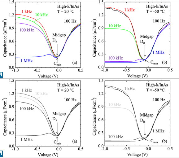
Field-Effect Mobility of InAs Surface Channel nMOSFET With Low Dit Scaled Gate-Stack
Frequency (100 Hz ≤ f ≤ 1 MHz) and temperature (-50 ≤ T 20 °C) characteristics of low interface state density D it high-κ gate-stacks on n-InAs have been investigated. Capacitance-voltage (C-V) curves exhibit typical accumulation/depletion/inversion behavior with midgap D it of 2 × 10 11 and 4 × 10 11 cm -2 eV -1 at -50 °C and 20 °C, respectively. Asymmetry of low-frequency C-V curves and C-T dependence for negative voltage showing a sharp transition of ≅-20 dB/decade between low- and high-frequency behavior indicate surface inversion. An inversion carrier activation energy and an InAs hole lifetime of 0.32 eV and 2 ns have been extracted, respectively. Surface channel nMOSFETs with gate length L g = 1 μm, channel thickness = 10 nm, and equivalent oxide thickness (EOT) 1 ≤ EOT ≤ 1.6 nm have been fabricated. For EOT = 1 nm, a subthreshold swing S = 65 mV/decade, transconductance g m = 1.6 mS/μm, and ON-current I ON = 426 μA/μm at an OFF-current I OFF = 100 nA/μm (supply voltage V dd = 0.5 V) have been measured. Peak electron field-effect mobilities of 6000-7000 cm 2 /Vs at sheet electron densities of 2-3 × 10 12 cm -2 were obtained for EOT as small as 1 nm.
Germanium n-Channel Planar FET and FinFET: Gate-Stack and Contact Optimization
We demonstrate Ge enhancement-mode nMOS FinFETs fabricated on 300-mm Si wafers, incorporating an optimized gate-stack (interface trap density D it below 2 × 10 11 eV -1 · cm -2 ), n + -doping (active doping concentration Nact exceeding 1 × 10 20 cm -3 ), and metallization (contact resistivity Pc below 2 × 10 -7 Ω · cm 2 ) modules. A new circular transmission line Pc extraction model that captures the parasitic metal resistance is proposed. At a supply voltage VDD of 0.5 V, 40-nm-gate-length FinFET devices achieved an ON-performance ION of 50 μA/μm at an OFF-state current IOFF of 100 nA/μm, a subthreshold swing S sat of 124 mV/decade, and a peak transconductance g m of 310 μS/μm. The same gate-stack and contacts were deployed on planar devices for comparison. Both FinFET and planar devices in this paper achieved the highest reported g m /S sat at VDD = 0.5 V to date and the shortest gate lengths for Ge nMOS enhancement-mode transistors.
Logic
High Mobility Channel
Silicon has been the transistor channel material of choice throughout all CMOS technology generations up until our 7nm node. TSMC’s 5nm technology is the first advanced logic production technology featuring SiGe as the channel material for p-type FinFET.
TSMC is actively exploring alternative transistor channel materials as an additional degree of freedom in the design of high performance and low power devices. Silicon-germanium and germanium are examples of TSMC’s exploratory research work, which has been extensively published and in some cases recognized as highlights in international conferences.
Sort by:
1-10 of 30
1


